

Multi-beam multi-column system
Description of “Multi Axis PSB”
1. Aims of Multi Axis PSB(Programmable shaped beam)
| ITRS Road map: " Optical lithography does not foresee a smaller than 10nm." | ⇒ EB lithography |
|---|---|
| Reproducibility and stability of the process at the time of miniaturization | ⇒ Multi-beam (PSB) |
| Throughput:10wph/module, 100wph / cluster | ⇒ Multi Axis (Multi-column) |
| Manufacturing of MEMS devices that cannot be flattened, multi-product mass production | ⇒ EB exposure Multi-column Multi beam |
| Large-scale production of wide variety of IoT device and analog unit | ⇒ EB exposure Multi-column Multi beam |
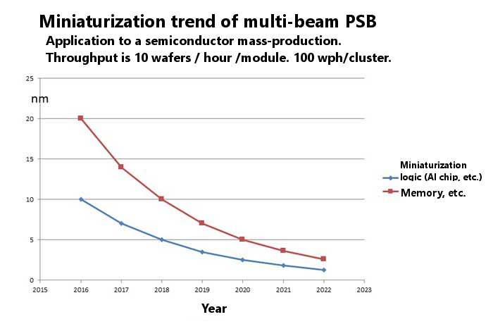
| Miniaturization and large-scale production of wide variety of Memory flash (20,10nm less) | ⇒ Multi column Multi beam |
| Logic device | ⇒ Multi column Multi beam |
| AI (artificial intelligence) device, 7~5mm less: Large-scale production of wide variety | ⇒ Multi column Multi beam |
■Promotion of miniaturization and Mask Less Lithography
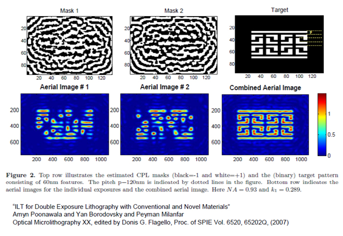
■Simplification and short TAT of Lithography: An example of the complexity of the pattern simplification and optical lithography: Double Exposure
2.Technology summary of Multi Axis PSB
Multi-column(Multi Axis)
Multiple Implementing of a small column with a drawing range of 26mm × 33mm
Multi-beam(PSB)
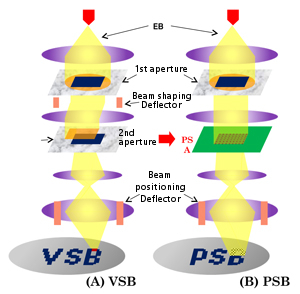
Multi–beam (PSB) Programmable Shaped Beam
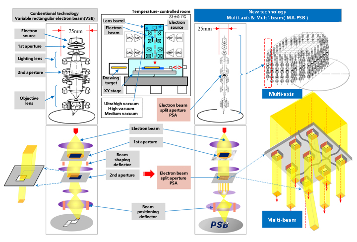
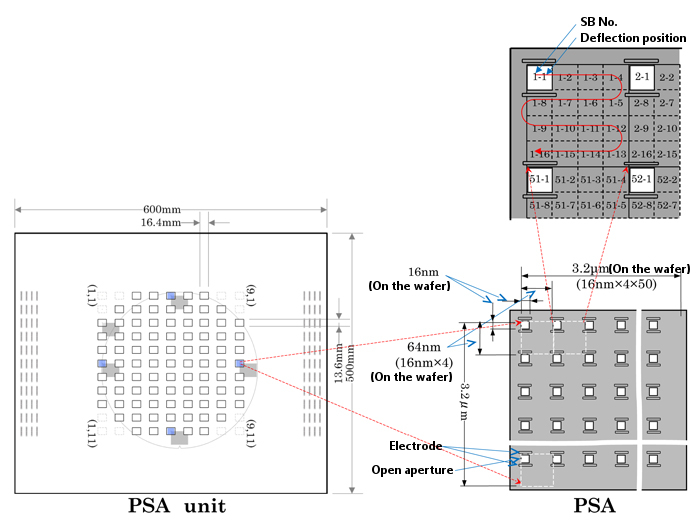
In an electron beam column at the position of second aperture of conventional type of variable shaped beam in which technology two square apertures are used, an active PSA(Programmable Shaping Aperture)device is set.
The PSA device has been made of three layers. First layer is made of silicone membrane. In this membrane there are square holes opened and arranged in the square lattice. Each hole size is for example four micron.
The pitch of the lattice for example 16 micron. The number of holes are 50 times 50 for example. So 2500 holes makes 2500 beams. They have all same square cross sections. The distance between each square center of beam is 16 micron in X direction and 16 micron in Y direction. The beams move along Z direction.
The second layer of PSA is miniaturized deflectors that make beams individually turn on and off.
The third layer of PSA is wiring layer on which 2500 wirings carry signals of 5 volts for individual beam turned on and off.
The beams travel through a demagnification lens and objective lens. The beams are reduced to size of 16 nm square and pitch is 64 nm. The size of total beams is 3200 nm square. Reduction ratio in this case is 250.
The beam positioning deflectors inside the projection lens deflect the beams by step of 3200 nm.
During exposure of one shot of 2500 beams movement of stage is chased by the beams according to trucking signal of deflectors, so that beams shot is very stable during exposure and resolution is kept to finest.
3.Module and cluster
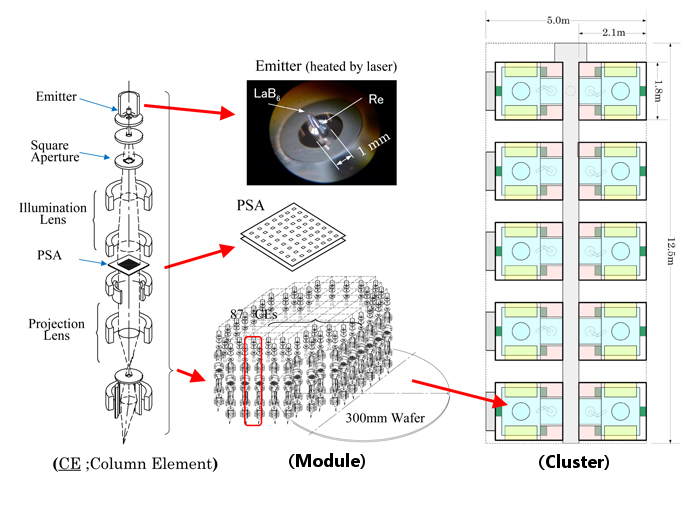
4.PSA
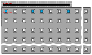
PSA(Programmable Shaping Aperture) device is set at the position of the second square aperture of conventional variable shaped beam column in which two square apertures are used. The PSA device makes 2500 square beams that 50 beams are arranged in X direction and 50 arranged in Y direction. They constitute a square lattice of size of 3200 nm on the objective plane. Each square beam has a size of 16 nm.
The distance between each beam is 64nm for example. Each beam goes through deflector electrodes, and is made turned on and off individually by the deflector electrodes.
In the following schematic the exposure method with the PSA is shown.
The beam positioning deflector which is located in the objective lens deflects the beam from 1-1 position,1-2,1-3,1-4,1-5,1-6,1-7,1-8,1-9,1-10,1-11,1-12,1-13,1-14,1-15 and to 1-16. The square region is exposed by beams and the beam on/off signal is applied to individual blanker at the PSA according to pattern data. After 16 sites were exposed then 3200 nm beams go to next 3200 nm square region.
If there is no on- data of all 2500 beams, the position for example 1-9 can be neglected to be exposed. Therefore the time for exposure can be small for sparse pattern.
We can expose efficiently with PSA by choosing various parameters according to generation of device pattern rule. The number of beams, size of beams, current density and number of columns are selected adequately to maximize the throughput of exposure system for various devices and generations.
5.PSB pattern drawing method
Drawing pattern:This pattern by micro-square lattice pixel can be represented by an integer multiple of the pitch of the square lattice size.
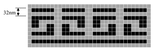
(An example of a drawing pattern:Half Pitch 16nm)
Throughput
Condition
| Resist sensitivity | 120μC/cm2 |
|---|---|
| Current density | 400A/cm2 |
| Latency for PSA deflection settling | 50ns |
| Latency for sub deflection settling | 85ns |
| Latency for main deflection settling | 200ns |
| Overhead time | 61.2s |
Wafer exchange etc.
| Module | 10.1wph (Full drawing) 16.1wph (The above drawing example) |
|---|---|
| Cluster | 101wph (Full drawing) 161wph (The above drawing example) |
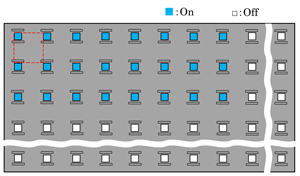
Examples of drawing operation:Deflection position 1 (1,2 -4,9-12,15,16)
6. PSB roadmap
Pattern size and PSA
- PSA can respond to the miniaturization and various device patterns by changing the aperture diameter and a numerical aperture.
- Even if you change device generations and pattern size, by increasing the data transmission rate in accordance with the numerical aperture, it is possible to maintain the throughput of 10wph at least.
* Relationship of the opening diameter of the pattern generation and PSA.
7.Merit of Multi Axis PSB
- We have adopted the vector scanning. For the shot in the stamp method, the vector scanning compared with the raster scanning is a good accuracy. Scanning direction and non-scanning direction of the precision and sharpness of the edge does not change.
- Cell Projection beam unlike conventional can be change free electrically.
The individual element beam count is 10000 from 2500. - In the 1-to-1 line-and-space, it can be drawn in half time.
- In the 1-to-1 hole pattern, it can be drawn in one quarter time.
- Uniform irradiation performance:It use the TFE electron gun that having a flat surface.
- The size pitch of the square lattice matrix beam group of PSA and the device pattern of PSA are match when drawing accuracy and high throughput is maximized.
- The size pitch of the square lattice matrix beam group of PSA and the device pattern of PSA are not match when throughput is degradation.
- You get a good production process, by using a PSA suitable for the production of the device pattern.
